Introduction:
Transistors have two different applications; they are used as:
- Amplifier (think of an audio amplifier)
- Switch (a transistor can switch high power very quickly and is used in, among other things, control units in the car).
Transistors are controlled by current. In, for example, microprocessors, the current must be kept as low as possible because of heat generation. In those, the MOSFET is often used.
There are two types of transistors, namely the NPN and the PNP transistor. These are described below.
NPN transistor:
The B stands for “Base”, the C for “Collector” and the E for “Emitter”.
With the NPN transistor, the arrow points away from the transistor. This transistor is often used when it is a “ground-side switch”, where the Emitter is connected to ground.

PNP transistor:
With the PNP transistor, the arrow points towards the transistor. A handy mnemonic for PNP is therefore “Pijl Naar Plaat” (arrow towards the plate).

Operation of the transistor:
In automotive engineering the transistor is most often used as a switch, so we will now go into that in more detail. We take an NPN transistor as an example.
In the figure the base is on the left, the collector on top and the emitter at the bottom. When a base current starts to flow (blue arrow), it follows its path to the emitter. As a result, a collector current also starts to flow to the emitter. As soon as the base current disappears, the current from collector to emitter also stops.
If half the base current flows, then also half the current (compared to I max.) flows. It is therefore clearly visible that the current switched by the transistor (from C to E) is completely dependent on the magnitude of B.
A transistor always has voltage drops due to the PN junction. Between the base and emitter this is 0.7 volts and between the collector and emitter 0.3 volts.
The transistor as a switch:
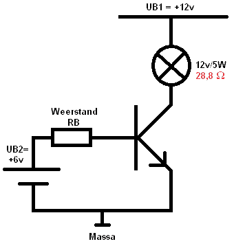
In the following example, a 12 volt / 5 watt lamp is controlled by a transistor. The voltage of UB1 (voltage source 1) is the battery voltage of 12 volts. The lamp is switched on the ground side. The base of the transistor is driven by UB2; “voltage source 2” of 6 volts.
The voltage drop between collector and emitter (UCE) is 0.3 volts, and between base and emitter (UBE) 0.7 volts. We will see this again in the calculation below. The gain factor is set to 200. This can always vary. The gain factor is the ratio between the base current and the collector-emitter current.
A circuit must always be implemented with a certain resistor (RB in the schematic above). If this resistor were not present, the transistor would fail immediately. The value that resistor RB must have depends on all factors; namely the voltages on both UB1 and UB2 and the required current for the components (resistors or lamps), etc. We will now calculate the load resistor RB.
To calculate the load resistor RB, the resistance of the lamp must first be calculated.
Now that the resistance RL is known, the collector current (IC) can be calculated.
UCEsat stands for “saturation”, in other words: saturation. As soon as the transistor conducts, a voltage drop of 0.3 volts occurs between points C and E (collector – emitter).
The next step is to determine the base current (IB):
For every transistor circuit there is a safety margin (IBK) of 1.5 x IB. So the value of IB must be multiplied by 1.5 once more. The reason for this will be explained later.
The base current is only 12% of the collector-emitter current. It is now clearly visible that a transistor can turn a small base current into a large main current.
Now that all currents in the schematic are known, resistor RB can be calculated.
UBE is the voltage between the base and the emitter. Due to the conductive material in the transistor there is always a voltage drop of 0.7 volts between points B and E.
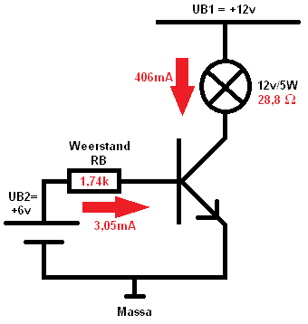
There are no standard resistors that are exactly 1.74k (kilo-ohms). So a standard resistor with a different value must be chosen. The choice must be made from the available resistors in the E12 series.

The required resistance of 1.74k lies between 1.5k and 1.8k. In that case, the lower resistance value must be chosen; 1.5k. This is to ensure that ageing and wear of the components have no influence on the currents in the circuit.
The transistor as an amplifier:
The transistor can be used as an amplifier. The base current can be changed by turning a potentiometer. By varying the base current, the amplified voltage, and therefore the voltage across the collector-emitter, is changed.
Transistor characteristic:
A characteristic curve can be made of an NPN transistor, see the figure below:
1st quadrant (top right) = UCE – IC
Up to 0.3 volts the line rises diagonally. This area is UCEsat (saturation of the transistor). After that the line runs almost horizontally.
2nd quadrant (top left) = IB – IC
Here the relationship between UB and IC is shown. IC = HFE x IB, with HFE = 10 in this characteristic, so IC is 10 times larger than IB. The safety factor of IB = 1.5 x IBK has not yet been included here.
3rd quadrant (bottom left) = UBE – IB
The voltage drop between the base and emitter of a transistor is the threshold voltage of a diode. The threshold voltage is 0.7 volts. From this voltage the transistor starts to conduct and the base current IB begins to flow. This too can be derived from the characteristic.
Example circuit with a characteristic:
Now it is time for a (simple) example circuit with a corresponding transistor characteristic. Here IB = 1.5 x IBK is included, which results in a horizontal line on the IB axis. In the circuit below, UB1 is the battery voltage and UBE (base-emitter voltage) comes from a switch or signal in a control unit. To calculate the current at UBE, the current IC (collector current) must first be calculated;
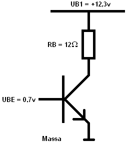
We now know that a current of 15 mA has to flow into the base of the transistor in order to make the transistor (with the given UB1 and RB) fully conduct, including the safety factor. The characteristic can then be filled in:
In this characteristic it can be seen that IB (current at the base) increases up to 10 mA. This part, from 0 to 10 mA, is calculated with the formula: IB = IC : HFE. The line then runs completely horizontally from 10 to 15 mA. This part is the gain factor of 1.5 (from the calculation of IB = 1.5 x IBK). With a base current of 15 mA, a collector current (IC) of 1000 mA flows.
Transistors are controlled by current. In, for example, microprocessors, the current must be kept as low as possible because of heat generation. In those, the MOSFET is often used.
Darlington transistor:
A control unit sends a base current to the transistor. A transistor can be driven into conduction by a control unit with a current of 0.1 to 0.5 mA. When we want to control an actuator that requires a high current, the ECU cannot supply the required current for the transistor. The primary current of an ignition coil is approximately 8 amperes. The control current will have to be amplified in order to bring the transistor into conduction. This presents a problem: the microprocessor cannot supply the desired current for the transistor.
By means of a Darlington transistor, a large current to the actuator can be switched with a small control current from the ECU.
The Darlington transistor consists of two transistors connected together in one housing.
The collector-emitter current of T1 provides the base current of T2. This results in a high gain factor, because the gain factors of both transistors can be multiplied together.
A very small base current of T1 (only a tenth of a milliampere) is often enough to bring T2 into conduction.
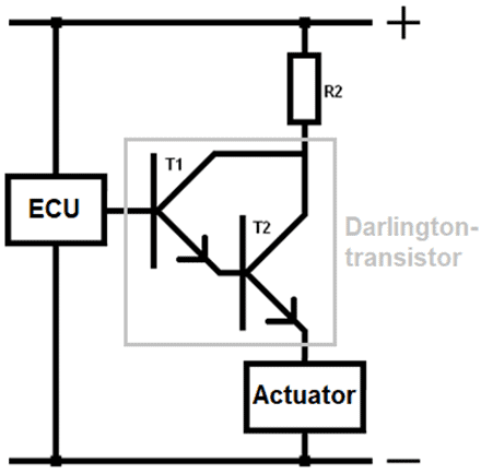
The current gain factor (Hfed) of the Darlington transistor is usually between 1000 and 10,000. The formula for calculating the gain factor of a Darlington transistor is:
Hfed = Hfe1 * Hfe2
- Advantage: thanks to the large current gain factor (Hfed), a small control current is sufficient to bring the Darlington transistor into conduction;
- Disadvantage: the base-emitter voltage of the Darlington circuit is twice as high as that of a single transistor. The voltage drop across the Darlington transistor is therefore considerably higher than that of a single transistor.
In the paragraph “Output signals” on the Interface circuits page, examples and applications of the Darlington transistor are described.
Related page: